Bluetooth Module: How to Level Shift 3.3V to 5V
In Bluetooth hardware design, it is often encountered that 1.8V, 3.3V, 5V, etc. used by module pins, 3.3V, 5V, etc. used to connect external interface chips, must be level-shifted due to level mismatch. If the power supply voltages of the two devices are different, for example, one is 3.3V and the other is 5V, then working under the condition of mismatched levels will cause signal transmission errors; if the voltage difference between the two is large, serious damage may occur. Bluetooth module.
In the design of Bluetooth module, how to Level Shift 3.3V to 5V? There are some methods for the module design:
1. Transistor composition level conversion method
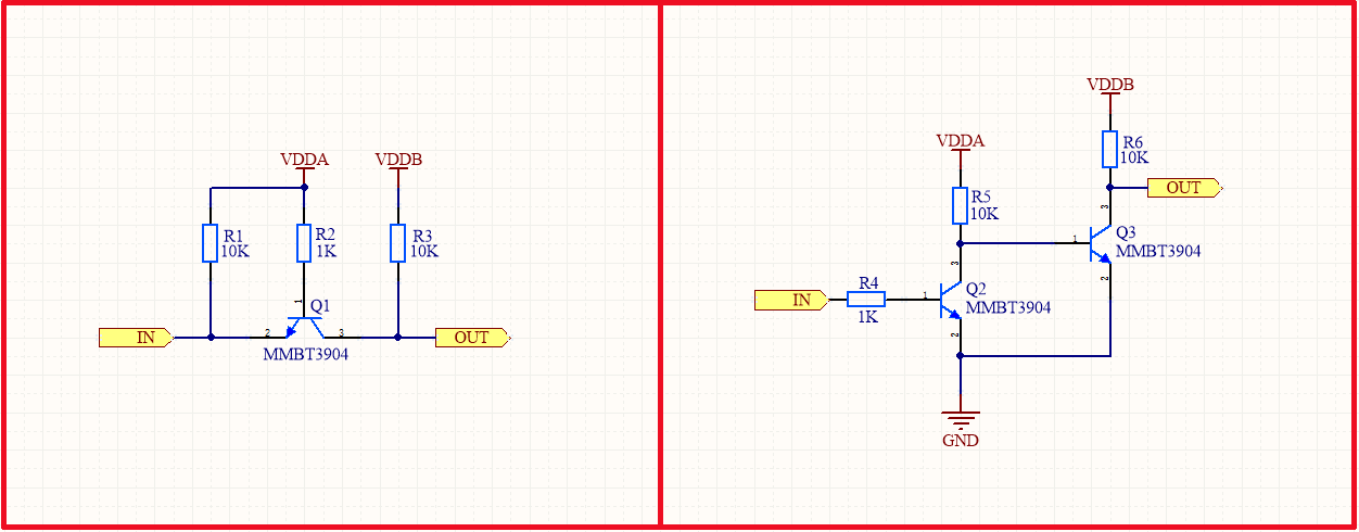
Figure 1
Working Principle:
The realization principle of the left picture of Figure 1: the left IN is the input, the right OUT is the output, and VDDA and VDDB are two different voltage domains that are converted to each other. When IN inputs 0V, transistor Q1 is turned on, and OUT is pulled down to a level close to 0V to achieve low-level conversion; when IN inputs high level VDDA, transistor Q1 is turned off, and OUT is pulled up to VDDB by resistor R3, so as to achieve high-level conversion. This circuit is a one-way conversion circuit, and the conversion direction is IN input and OUT output.
The realization principle of the right picture in Figure 1: When the input IN is at a low level, the transistor Q2 is turned off, the transistor Q3 is turned on, and the output OUT is pulled low, thus realizing low-level conversion; when the input IN is at a high level VDDA, the transistor Q2 It is turned on, so that the transistor Q3 is pulled low and turned off, so that the output OUT is pulled up to VDDB by the resistor R6, thereby realizing high-level conversion. This circuit can only realize the left IN input and the right OUT output, and cannot be reversed.
Note: The purpose of using two triodes in the right picture of Figure 2 is to keep the input and output signals in phase. If inversion is acceptable, one triode can also be used.
Advantages:
(1) Cheap: triodes are common and easy to purchase, and the price is low.
(2) Strong driving ability: The driving ability depends on the triode, which can achieve tens of mA;
(3) Low leakage current: The leakage current between IN and OUT is small (uA level), almost negligible.
Disadvantages:
(1) Speed: The two-stage triode is a current-driven type, plus the circuit and parasitic capacitance, the converted waveform is not very ideal. Generally, it can only be used for signal conversion within 100K.
(2) Many devices: In-phase conversion requires 2 triodes and matching resistors, which takes up a lot of space during multiplexing.
Application:
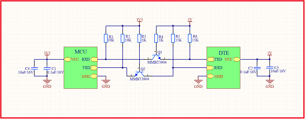
Figure 2
Figure 2 is a one-way serial level conversion circuit. The implementation principle is as follows: the RXD interface of the Bluetooth module receives data, and when the TXD interface of the terminal device outputs data, 3.3V and 5V are two different voltage domains that are converted to each other. When the TXD interface of the terminal equipment outputs 0V, the transistor Q1 is turned on, and the RXD interface of the module is pulled down to a level close to 0V to realize low-level conversion; when the TXD interface of the terminal equipment outputs a high level of 5V, the transistor Q1 is turned off. The Bluetooth RXD interface is pulled up to 3.3V by the resistor R1 to achieve high-level conversion. Similarly, the TXD interface of the Bluetooth module outputs data, and the RXD interface of the terminal device receives data to realize the conversion from 3.3V to 5V.
2. Bidirectional level conversion method composed of MOS tube
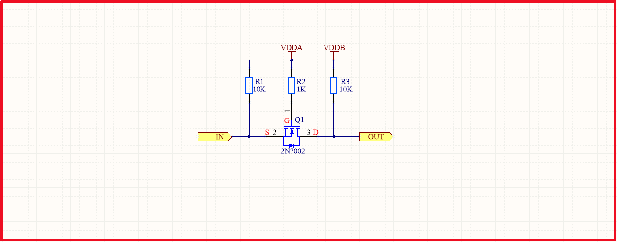
Working Principle:
When the IN terminal outputs a high level, the Vgs of the MOS transistor Q1=0, the MOS transistor is turned off, and the OUT terminal is pulled up to VDDB by the resistor R3;
When the IN terminal outputs a low level, the Vgs=VDDA of the MOS transistor Q1 is greater than the turn-on voltage threshold, the MOS transistor is turned on, and the OUT terminal is pulled down to a low level through the MOS transistor;
When the IN terminal outputs a high-impedance state, the MOS tube is turned off, and the OUT terminal is pulled up to VDDB by the resistor R3;
When the OUT terminal outputs a high level, the Vgs of the MOS transistor Q1 remains unchanged, the MOS transistor remains off, and the IN terminal is pulled up to VDDA by the resistor R1;
When the OUT terminal outputs a low level, the MOS tube Q1 is not turned on, and the MOS tube first pulls the IN to a low level through the body diode. At this time, Vgs≈VDDA, the MOS tube is turned on, and the voltage of the IN terminal is further pulled down;
When the OUT terminal outputs a high-impedance state, the Vgs of the MOS transistor Q1 remains unchanged, the MOS transistor remains off, and the OUT terminal is pulled up to VDDB by the resistor R3;
Notice:
(1) In normal operation, VDDB>=VDDA;
(2) Vgs<=VDDA; Vds<=VDDB;
(3) The low-level threshold of the IN terminal is greater than about 0.7V (depending on the diode voltage drop in the NMOS).
Advantages:
(1) It is suitable for low-frequency signal level conversion, and the price is low.
(2) After being turned on, the voltage drop is smaller than that of the triode.
(3) Forward and reverse bidirectional conduction, which is equivalent to a mechanical switch.
(4) Voltage type drive requires a certain drive current.
Application:
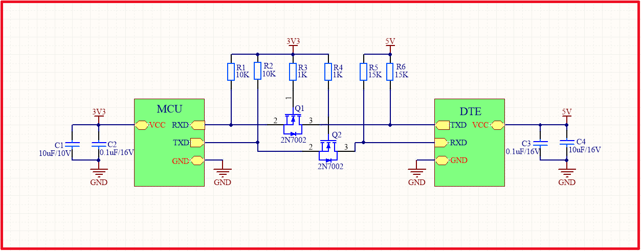
Working Principle:
When no data is sent on the bus: neither side actively pulls down the bus, so the MOS tube is also not turned on, all because of their respective pull-up resistors, the left side is high level 3.3V, and the right side is high level 5V.
When Bluetooth needs to send data 1 to the terminal device: that is, the microcontroller TXD is at a high level of 3.3V, the Vgs of the MOS transistor Q2 is 0, the MOS transistor Q2 is turned off, and because of the presence of the pull-up resistor on the right side, the terminal device RXD interface level remains at 5V. It can be considered that the Bluetooth module normally sends the data 1 to the terminal device.
When the module needs to send data 0 to the terminal device: that is, the Bluetooth TXD is low level 0V, the Vgs of the MOS transistor Q2 is 3.3V, the MOS transistor Q2 is turned on, the right level is the same as the left level, and the terminal device RXD interface is low. Flat 0V. It can be seen that the Bluetooth module normally sends data 0 to the terminal device.
When the terminal device needs to send data 1 to the Bluetooth module: that is, the terminal device TXD is at a high level of 5V, and the module RXD does not actively pull the low level, so the MOS tube Q1 is not turned on, and the left side maintains the pull-up level of 3.3V. It can be seen that the terminal device normally sends the data 1 to the Bluetooth.
When the terminal device needs to send data 0 to the Bluetooth module: that is, when the terminal device TXD is at a low level of 0V, because of the existence of the diode in the MOS tube Q1, the diode in the tube is turned on, the S pole of the MOS tube Q1 is pulled down, and Vgs is close to 3.3V, the MOS transistor Q1 is turned on, so that the left and right levels are close to 0V. It can be seen that the terminal device normally sends data 0 to the module.
Notice:
(1) Access method of MOS tube: The S pole of the MOS tube should be connected to the low power supply side and cannot be reversed.
(2) Selection of MOS tube (the turn-on voltage of MOS tube needs to be paid attention to): The turn-on voltage threshold of MOS tube (the maximum value in Vth(GS)) needs to be less than the low power supply voltage.

Figure 4
Figure 4 is a partial parameter table of the NMOS tube of 2N7002, 1V<Vgs<2.5V. If there is mutual conversion between 5V and 3.3V, this MOS tube can be used. But if it is inter-conversion between 3.3V and 1.8V, this tube cannot be used. Because the turn-on threshold voltage is 1~2.5V. Because a device with a turn-on voltage greater than 1.8V may be used, the MOS tube may never be turned on.
(3) Low level means equal to or close to 0V; high level means equal to or close to the power supply voltage. Therefore, the high level of the device in the 3.3V voltage domain is equal to or close to 3.3V; the high level of the device in the 5V voltage domain is equal to or close to 5V. For specific requirements, see how the data sheet of the chip explains this limited range. Commonly, for example, 0.3 times the "chip power supply voltage" and below are low levels, and 0.7 times the "chip power supply voltage" and above are high levels. That is to say, when the "chip supply voltage" is 5V, 5 x 0.3 = below 1.5V is low level, and 5 x 0.7 = above 3.5V is high level.
3. One-way level conversion circuit composed of diodes
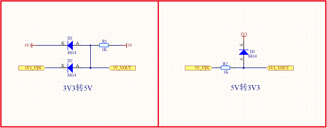
Figure 5
Working Principle:
As shown in Figure 5, the diode clamping method is used for level conversion. The left picture in Figure 5 is 3.3V to 5V. When the 3V3_VIN level is high, 5V_VOUT=3.3V+Vd(D2)=3.3+0.7≈4V, reaching the high level threshold of 5V, when the 3V3_VIN level output is low When the 5V_VOUT output voltage is about =Vd(D2)≈0.7V, it is within the low-level threshold range.
The right picture in Figure 5 is 5V to 3.3V, when 5V_VIN input is high level, 3V3_VOUT=3.3V+Vd(D3)≈4V, when 5V_VIN input is low level, 3V3_VOUT=0V.
Advantage:
(1) Small leakage current: Since the leakage current of the diode is very small (uA level), it can prevent the power supply from being backflowed in one direction, preventing the backflow of 3.3V to 5V.
(2) Easy to implement: diodes and resistors are easy to purchase and occupy a small area.
Shortcoming:
(1) Large level error: The main reason is that the forward voltage drop of the diode is large, which is easy to exceed the working voltage range of the chip.
(2) One-way backflow prevention: it can only prevent backflow in one direction, but cannot prevent backflow in both directions.
(3) Unsatisfactory speed and driving ability: Due to the resistance current limit, the driving speed and ability are not ideal, and can only be applied to frequencies within 100K.
Application:
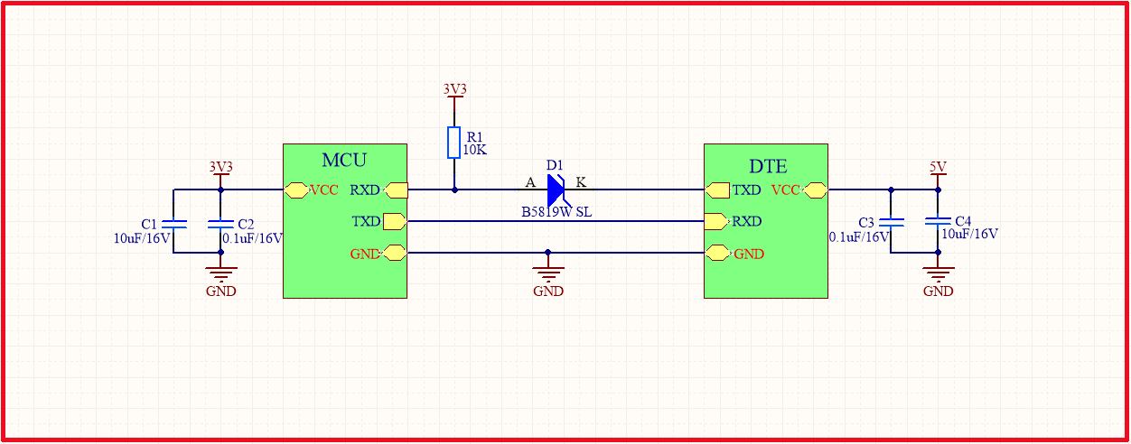
Figure 6
Working Principle:
As shown in Figure 6, the RXD of the Bluetooth is 3.3V, and the TXD of the terminal device is 5V. When the terminal device outputs a 5V signal, the diode D1 is blocked, and the RXD is pulled to the acceptable 3.3V level of the module through the pull-up resistor R1; when the terminal device output is low, the diode D1 is turned on, and the RXD is pulled through the diode to the level of 3.3V. Low level, but the low level at this time is the forward voltage drop of the diode, and this value must be within the low level range that the module can recognize.
Notice:
(1) The terminal equipment RXD and the module TXD are directly connected, so the minimum threshold of the high level that the terminal equipment can recognize should be less than or equal to 3.3V.
(2) The maximum low-level threshold that the Bluetooth module can recognize should be greater than or equal to the diode’s tube voltage drop.
(3) Considering the communication rate and the low-level voltage amplitude, the diode uses a high-speed Schottky diode, and the VF is as small as possible.
4. Bidirectional level conversion circuit composed of level conversion chip
Figure 7
Working Principle:
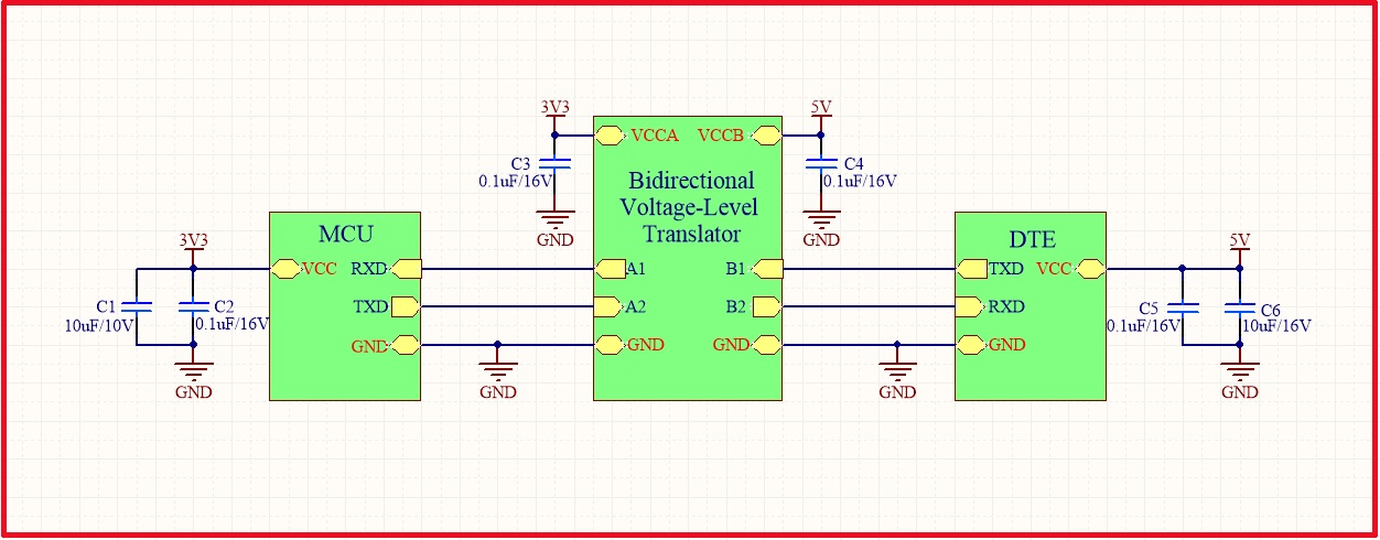
As shown in Figure 7, a dedicated level conversion chip is used for level conversion. The level conversion chip provides convenience for data communication and control between different voltage domains. For example, the chip TXB0102, as a bidirectional level conversion chip powered by dual power supply, judges the conversion direction by detecting the driving current of the external port, so it does not need an external direction control pin to select the direction of the control device conversion. Therefore, it is very easy to use it, and the software does not need to consider changing its conversion direction.
Advantage:
(1) Strong driving ability: The output of the special chip generally uses the CMOS process, and the output current can reach tens of mA.
(2) The leakage current is almost 0: there are some amplifiers and comparators inside, and the input impedance is very high, generally reaching hundreds of K; the leakage current is basically nA level.
(3) The number of channels is large: special-purpose chips are available for different applications, ranging from 2 channels to dozens of channels, which are very suitable for occasions with high area requirements.
(4) High speed: Due to the high integration level and high technology of special chips, the speed can be done from hundreds of KB to several MB.
5. Level conversion circuit composed of resistor divider
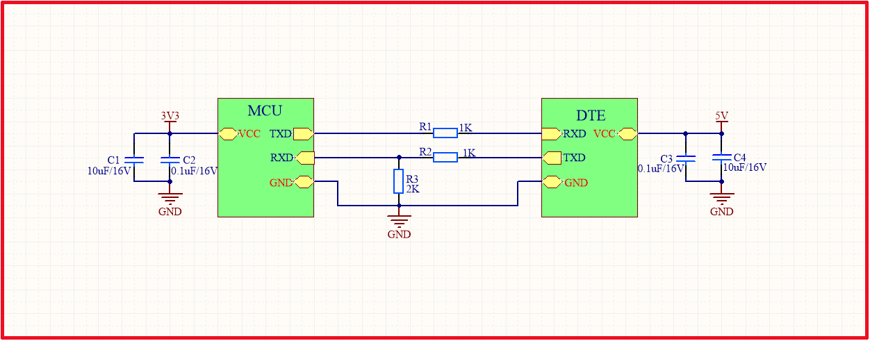
Figure 8
Working Principle:
As shown in Figure 8, R2 and R3 form a voltage divider. In the figure, the RXD port voltage=5V*2K/(1K+2K)≈ \approx≈ 3.3V. There is no voltage divider directly between the TXD of the Bluetooth module and the RXD of the terminal device, only a resistor is added to limit the current.
Note:The minimum high voltage threshold of the terminal equipment should be less than or equal to 3.3V.
Advantage:
(1) Cheap: cheap is the biggest advantage, 2 resistors are less than a penny;
(2) Easy to implement: The resistors are easy to purchase and occupy a small area.
Shortcoming:
(1) Speed: In order to reduce power consumption, the voltage division method uses resistors above K level, plus the distribution and parasitic capacitance of circuits and devices, the speed is difficult to increase, and generally can only be applied to frequencies within 100K.
(2) Driving ability: Due to the use of a large resistance resistor, the driving ability is strictly controlled, which is not suitable for occasions requiring high driving ability, such as LED lights.
(3) Leakage: Leakage is the biggest disadvantage of this solution. Due to the direct connection through the resistance, the voltages at the left and right ends will flow, thus affecting each other.
6. Level conversion circuit composed of resistor current limiting
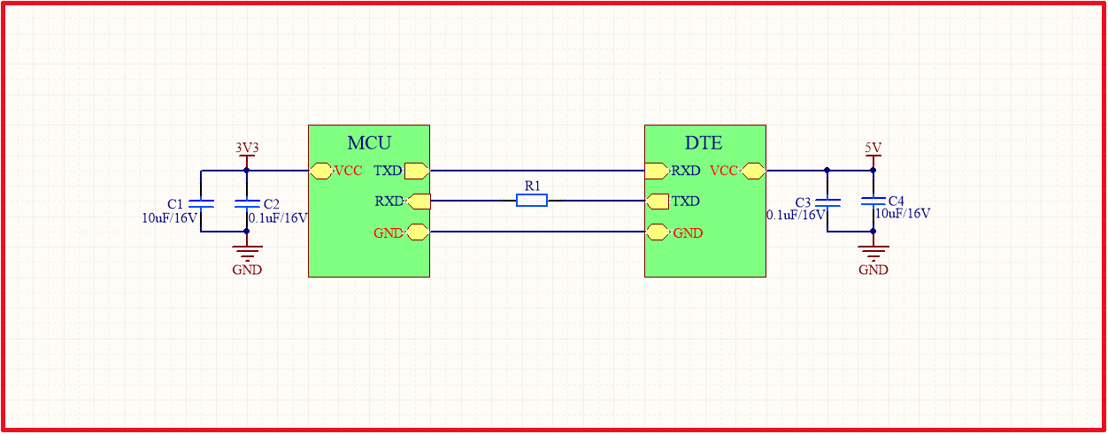
Figure 9
Working Principle:
As shown in Figure 9, a resistor current limiting method is used to realize the conversion between two different levels. The specific practical principle is that the input current of the module does not exceed a certain value. For example, the input current value of the terminal equipment used cannot exceed 20mA, which can be considered as safe. If it is 5V to 3.3V, the resistance R1>(5-3.3 V)/20mA=85Ω, choosing a 1K resistor is considered safe. Because the inside of the module can be equivalent to a load resistance RL, which forms a voltage division relationship with R1.
Advantage:
(1) Cheap: Cheap is the biggest advantage, and it can be solved with only one resistor.
(2) Easy to implement: The resistors are easy to purchase and occupy a small area.
Shortcoming:
To use the resistance current limiting method, you need to be very familiar with the internal structure of the Bluetooth module, and also consider the voltage range after current limiting.
Summary
The above several level conversion methods are relatively common methods, and the level conversion mainly considers the following aspects:
(1) Level matching: This is the premise, and the converted level needs to be within the acceptable range of the other party.
(2) Leakage current: Not only should the levels be matched between the two, but the leakage currents should not affect each other. Using diode level conversion for RS485 output may cause leakage current of external devices to affect the startup of internal devices, and the internal devices output a bunch of garbled characters when they are started, affecting the normal operation of the other party.
(3) Driving capability: The driving capability should also be considered after the level conversion. For example, after the I2C level conversion, mounting multiple I2C devices requires consideration of the driving capability.
(4) Speed: In theory, all level conversions have speed sacrifices. The best speed solution is a dedicated level conversion chip, followed by a triode solution, and the worst is a resistor divider solution.
(5) Cost: In addition to considering the functional requirements in the circuit design, the cost should also be taken into account.
(6) Number of channels: A too complicated conversion scheme is not suitable for the case of multiple channels, and will occupy too much area.

